Microcontroller Architecture
A quick overview on Microcontroller architectures, Wendy Ju & Michael Gurevich
Contents
Microcontroller
A microcontroller is essentially a small computer on a chip. Like any computer, it has memory, and can be programmed to do calculations, receive input, and generate output. Unlike a PC, it incorporates memory, a CPU, peripherals and I/O interfaces into a single chip. Microcontrollers are ubiquitous, found in almost every electronic device from ovens to iPods.
Clock
The AVR has a clock that “ticks” at a regular rate. A variety of clocks types and speeds are available, including a built-in circuit or external crystals. We use a 16MHz external crystal oscillator for the maximum clock speed the AVR will run at. Note how much slower this is than a PC – and remember this when you write your code! Microcontrollers differ in the number of clock ticks it actually takes to execute an instruction. This is why we use the term MIPS or million instructions per second, to better describe the “speed” of a CPU. One feature of the AVR is that most instructions are executed in one clock cycle, therefore it runs at around 1 MIPS / MHz. Other microcontrollers running at 16MHz may have less MIPS.
Architecture
Computer architecture is a huge topic in itself. We will just develop a general picture of how the AVR microcontroller works. It has a Harvard architecture. This means that the program and data are stored in separate memory spaces which are accessible simultaneously. Therefore, while one instruction is being executed, the next one can be fetched. This is partly how one execution per clock cycle can be achieved. With other microcontroller architectures, there is only 1 way to access memory, so executions and program instruction access must be done alternately.
Program Memory
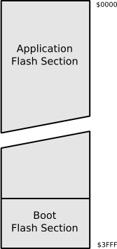
The AVR's program is stored in nonvolatile (persistent on power-down) programmable Flash memory. It is divided into 2 sections. The first section is the Application Flash section. It is where the AVR's program is stored. The second section is called the Boot Flash section and can be set to execute immediately when the device is powered up. The Flash has a special property of being able to write over itself, which may seem like a stupid thing to do.
But the Boot Flash section can come in handy if it is programmed with a small program that takes data from the serial port and writes it into the Application Flash section. Such a program is called a bootloader, and it allows the device to be programmed from a regular serial port, rather than using a complicated or expensive programmer circuit. For commercial devices, it makes so-called “firmware upgrades” very easy. We will use a bootloader. This program is already loaded on the chip.
Figure 1 - AVR's Flash Program Memory (after ATmega32 datasheet p. 14)
Hex Code
All the code you write is linked, assembled and otherwise compiled into hex code, (also known as byte code) which is a series of hexadecimal numbers that are interpreted as instructions by the microcontroller. The beauty of a high-level language like C is that you don't need to understand the details of the microcontroller architecture.
Data Memory
The AVR's data memory is volatile RAM. It is organized in 8-bit registers.
Registers
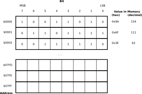
All information in the microcontroller, from the program memory, the timer information, to the state on any of input or output pins, is stored in registers. Registers are like shelves in the bookshelf of processor memory. In an 8-bit processor, like the one we are using, the shelf can hold 8 books, where each book is a one bit binary number, a 0 or 1. Each shelf has an address so that the controller knows where to find it. Some registers, such as those in RAM, are for storing general data. Others have specific functions like controlling the A/D converters or timers, or setting and getting values on the I/O pins. Registers in RAM can be read or written. Other registers may be read-only or write-only. In fact, some specialized registers may have certain bits that are only to be read, and certain bits that are only to be written.
Bits and bytes
One byte is made up of 8 bits, and there are 256 unique possible values for each byte. All the information in the microcontroller is stored in byte-size chunks; since it would be tedious to write out all the 1's and 0's in binary format, we represent each byte of information as a two-digit hexadecimal number. For example, 11110011 in binary=243 in decimal=F3 in hexadecimal. We usually write 0xF3 to clue people in that the numbers are in base 16. Memory address locations are normally given in hexadecimal, but with a preceding $ to indicate an address, as opposed to a value, eg $03DF. Note that with 4KB of RAM, we need 2 bytes to specify all the addresses for our processor.
Hint: Try typing "0xF3 in binary" and similar into the standard google search engine.
Figure 2 - Registers in RAM
Registers on the AVR Microcontroller
The data registers on the AVR, like the Flash program memory, are organized as a continuous set of addresses, but with different specialized sections. Unlike the Flash program memory, these different sections refer physically to completely different types of memory. The largest set of registers refer to the RAM. This is volatile memory for storing data such as variables or strings to be outputted.
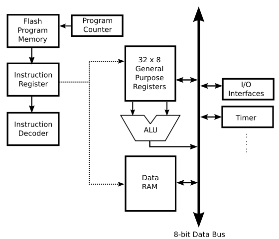
Another set of registers are the general-purpose working registers. There are 32 of these, and they hold a small amount of data which is directly acted on by the Arithmetic Logic Unit (ALU) when it performs calculations. When the program gives an instruction to add 2 numbers, these must be fed into the ALU from the working registers. If the numbers are in RAM, they must first be moved into the ALU. A good compiler will make sure that transfers from RAM to the working registers are minimized, because RAM access is generally slow.
The final set of registers have special functions for doing things like I/O, timing, or analog-to-digital conversion. All of these registers share a Data Bus to transfer data between them. The output of the ALU is also on this Bus, so that the results of instructions can be used to store new values in RAM, create output, put new values in the working registers or start a timer, for example. The data bus can carry 8 bits of information at a time.
IO Registers
In order to read and write to the input and output pins on the microcontroller, however, you will need to know a little about the input and output architecture. The reason that the IO pins are divided into ports of 8 pins is that this allows the state of the pins to be represented by 4 bytes, named PORTA, PORTB, PORTC and PORTD. Each physical IO pin corresponds to a logical bit on the port. The value of pin3 on Port D lives in slot 3 on the PORTD bookshelf.
Setting and Clearing IO
The term for assigning a logical high value (1) to a pin is setting, and the term for assigning a logical low value (0) is clearing. You can write to the IO registers one byte at a time, for example, by assigning the value 0xBB to PORTB, or by assigning one bit at a time, clearing PB2 (portB bit 2) and PB6, and setting the rest.
DDR Registers
Not all of the I/O registers are physical pins. Since the IO pins are configurable to be either input or output, the controller needs some place to store the directionality of each bit. These are stored in the Data Direction Registers. Like all the other registers, the DDRs have 1's and 0's, but its 1's and 0's indicate whether the corresponding port pin is an input (0) or output (1). This register acts as an I/O port librarian, controlling who is allowed to change the data on the shelves, bit by bit. So, if I set DDRA to 0xF0 (a.k.a. 1111 0000), this means that bits 7-4 on PORTA are set to output, and bits 3-0 are set to input. If PORTA was originally set to 0xFF (a.k.a 1111 1111) and I subsequently write 0xAA (a.k.a 1010 1010) to PORTA, I should read 0xAF on the PORTA.
Port Features
The pins on the different ports also have different features, much as each of the Superfriends had different super powers. For instance, PORT A can be bi-directional IO, but it can also be used for analog input. This functionality can be very useful for reading sensor data. To enable the switching between analog and digital inputs, a special register called ADCSR (Analog to Digital Control & Status Register) is needed; each bit in ADCSR sets some aspect of the AD operations. You do not need to set these bits explicitly, but you need to be aware that you should run the library commands (such as a2dInit())in the appropriate library (a2d.h) to tell the processor to set these registers. A more complete description of all the ports and their special magical powers can be found in the processor datasheet.
Figure 3 - AVR Architecture (after ATmega32 datasheet p. 6)
==Program Execution== - Hex Code is what is stored in the Flash Program memory. When the program runs, the hex code is accessed by the Program Counter. It loads the next instruction into a special Instruction Register. The operands of the instruction are fed into the ALU , while the instruction itself is decoded and then executed by the ALU.


